Johann's Carrier Board
| Website | More Info |
|---|---|
| More Info | GitHub Issue |
Description
Warning
Warning: I’m not an electrical engineer. Do not use this information/hardware unless you have verified the correctness beforehand. The described board is not considered finished work, but in development phase.
Idea and features
Originally, I just wanted to replace my aging NAS (ARMv5 CPU, 512 MB RAM, single 3 TB 3.5 inch SATA HDD) with a Raspberry Pi based solution. While plenty solutions already existed, none seemed perfect for what I wanted. Roughly, my requirements were:
- Gigabit Ethernet connection
- Fast and efficient mass storage connection; I ruled USB, because it would add overhead and latency: SSDs and HDDs do not have native USB connectivity, so USB always requires additional hardware and software components; also, the Raspberry Pi SoC doesn‘t have native USB3
- Reasonable enclosure
The only option for mass storage is basically the Raspberry Pi 4 SoC PCIe lane. So my very first idea was to use a mini-PCIe SATA board to connect my existing HDD. However, in the course of designing my new NAS, i learned that:
- mini-PCIe is now legacy and superseded by the M.2 standard.
- while M.2 SATA boards exist, native M.2 NVMe SSDs have reached a price range where I just could retire my 3 TB SATA HDD and replace it by a 4 TB NVMe SSD.
So the end result regarding mass storage was that I want an M.2 2280 slot into which I can insert an M.2 2280 NVMe SSD.
My other big concern was the availability of a reasonable enclosure. There is a huge amount of Compute Module 4 carrier boards out there, but for most of them no or at most one case is available. And for the boards with a case available, it would not provide space for the storage. Having looked at standard PC form factors, NUC (4x4 inches = 10.24x10.24 cm boards) seemed most appropriate to me, given that a 3.5 inch HDD (which I wanted to use originally) also has a width of 4 inches. Later, while searching the internet for „10x10 cm computer case“, I stumbled upon „extruded aluminum enclosures“ and stuck to these, as they are really broadly available from many manufacturers. Mounting holes for the NUC form factor are still present, but I do not expect them to fit any actual NUC case as I had to reduce the hole diameter to compensate for the board edge length reduction from 10.24 to 10 cm. In retrospect, I guess NUC would not have worked very well anyway, because the available cases do not seem to have a changeable back plate for the external connectors.
So the end result regarding enclosures was that I want the board to fit a 10x10 cm aluminum slide-in enclosure.
Having fulfilled by own requirements, I started thinking about what else fits on the 10x10 cm PCB (not using every square mm would be waste, right?). I ended up with the following feature set:
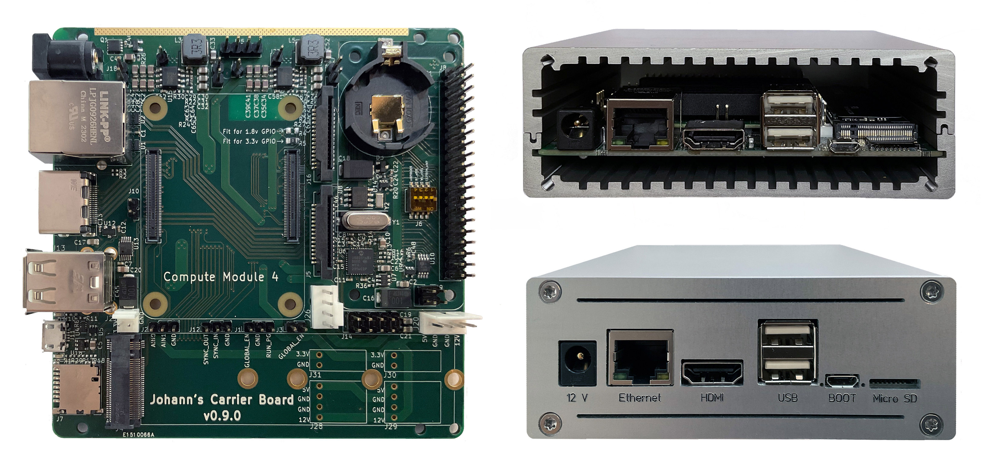
- 12V power jack (requires 5.5 x 2.1 mm plug) with integrated buck converters for CM4 (5V) and M.2 slot (3.3V)
- 1 Gigabit Ethernet port
- 1 HDMI port
- 2 USB-A ports (driven by internal 4-port USB hub)
- 1 Micro-USB-B port for RPI-BOOT (i.e. recovery only)
- 1 micro SD card slot (works with CM4-LITE only)
- 1 internal M.2 key M slot
- 2 internal USB ports (driven by internal 4-port USB hub)
- 1 internal 2-lane CSI port (Raspberry Pi 4 compatible?)
- 1 internal 2-lane DSI port (Raspberry Pi 4 compatible?)
- Internal RTC with 3022 coin cell battery holder
- Internal fan controller & connector
- Internal 4-pin “Berg” power connector providing 5V and 12V
- Internal 2-pin power connector providing 3.3V
- 40-pin standard Raspberry Pi GPIO header with mounting holes for Micro(!)-HAT
Compared to the official Raspberry Pi Compute Module 4 IO Board, the following features are different/missing:
- M.2 slot instead of PCIe slot
- Mounting holes and space for Micro-HAT instead of (full-size) HAT
- First CSI port has only 2 instead of 4 lanes
- First DSI port has only 2 instead of 4 lanes
- No second CSI port
- No second DSI port
- No second HDMI port
- Placement of CM4 on the carrier board is inappropriate for WiFi/Bluetooth
- Missing review of an electrical engineer
- Missing hardware validation and testing
- Missing regulatory compliance testing
Mechanical Design
All external connectors are on one side of the PCB. I really consider it annoying if cables come out from a device on several sides, because this is not what you want on a desk or in a rack.
The PCB should fit into many available 10x10 aluminum enclosures and I really like this solution as this makes the device robust and aluminum should also result in good heat dissipation. A disadvantage is of course that it also prevents using internal WiFi/Bluetooth antennas, but WiFi was never a design goal anyway.
As mentioned above, the board has some mounting holes on the same positions as NUC boards. However, these are smaller than usual, so I do not expect that the board can be properly mounted into a NUC case.
„Microbarbs“ (this seems to be a trademark, but I could not find a general term, as they seem to be pretty unique) are used as threaded inserts. These need to be pressed-in from the board bottom side, so that a M.2 standoff can be screwed in from the top side. This approach is probably not feasible for mass production, where a solderable standoff seems preferable. As solderable standoffs are a little larger than the Microbarbs, the M.2 slot needs to be placed a little more left, which then again requires a different microSD slot which allows placing it a little more left as well (as M.2 slot and micro SD slot are already located as close as possible to each other - this is one of the most critical points in the whole design, also impacting the PCB).
Almost all external connectors overlap the board edge by 2 mm, so that a 2 mm thick end plate has to be used for the enclosure in order to have the external connectors ending exactly flush to the enclosure. The two exceptions are:
- The micro USB connector overlaps the board edge by only ~1.6 mm, as I could not find a connector with the solder pads located in a way to allow moving it further over the board edge.
- The micro SD slot does not overlap the board at all as its solder pads do not allow this. I could not find a micro SD slot which allows for an overlap and also allows for the same card detection logic as on the official Raspberry Pi Compute Module 4 IO Board (see “Electrical design” section).
The 12V power jack requires a plug with an outer diameter of 5.5 mm and an inner diameter of 2.1 mm, which is pretty standard. On the other hand, 12V power supplies providing >=3A often have an inner diameter of 2.5 mm (with the outer diameter still at 5.5 mm). So I’m not really sure what is the best choice here.
Electrical design
The schematic is more or less a 1:1 copy of the official Raspberry Pi Compute Module 4 IO Board, with some components removed, the PIN headers changed and the PCIe slot replaced by an M.2 slot.
An M.2 slot is in general very versatile in that it can offer various electrical interfaces, including SATA, PCIe and USB. As my primary goal was a NAS, I chose to use PCIe only. And, as the Raspberry Pi 4 SoC only offers only one PCIe gen 2 lane, this is what is exposed via the M.2 slot (which generally allows exposing up to 4 PCIe lanes). This should be compatible with most (?) M.2 NVMe SSD drives, but the speed will be limited to the single PCIe gen 2 lane, which means a maximum gross data transfer rate of 500 MB/s, resulting in a net data transfer rate of <400 MB/s.
The other thing to note on the M.2 slot is that 3.3V are always applied to it, even if the Raspberry Pi SoC is not running. It is probably possible to add some circuitry to only power it when the Raspberry PI SoC is running, but I didn’t care.
The official Raspberry Pi Compute Module 4 IO Board uses an micro SD slot which has two pins for card detection (named DET_A and DET_B in the schematics). Inserting a micro SD card into the slot will basically just short-circuit these two pins so that you are free to design your schematic around this short-circuit. Many other micro SD slots only have one pin for card detection which will by design be short-circuited to 3.3V on card insertion. The official Raspberry Pi Compute Module 4 IO Board also controls the 3.3V supplied to the micro SD slot via a power switch (U18) so that the voltage is only supplied to the SD card slot when the CM4 does not pull SD_PWR_ON low. This means that the one pin card detection style mechanism could not work as long as SD_PWR_ON is low, possibly leading to a chicken-egg problem between “card detected” and “SD slot powered”. And finally, the official Raspberry Pi Compute Module 4 IO Board schematic marks the DET_A and DET_B card detection pins as “do not populate on PCB”, i.e. the whole card detection stuff seems currently unused. As I simply do not know what the Raspberry Pi engineers intended previously and intend in the future, I also chose a micro SD slot with two pins for card detection and kept the schematic the same. But anybody continuing the work on this carrier board should revisit this again, as the current micro SD slot choice not only prevents moving the slot left to overlap the PCB (as all other external connectors do), but also negatively impacts the position of the M.2 mounting holes on the PCB.
PCB
This carrier board is based on a 4 layer PCB stackup, where I used the inner layers for ground and the outer layers for signals and power. Components are only placed on one side of the PCB with the goal of keeping the production cost low. On the top and bottom of the PCB, a clearance of ~3 mm from board edge to components is kept, so that the board can be inserted into common aluminum enclosures which provide guided slots on their inner sides. On the top of the PCB, GND copper is exposed without solder mask. This might help cooling the power circuitry via the aluminum case, but I do not know if this really has an effect.
While the switching power regulators on the top of the board use the same schematics (!) as on the official Raspberry Pi Compute Module 4 IO Board, the PCB layout is different. Doing such layouts correctly requires a lot of knowledge and experience which I lack. So anybody who wants to further work on this board, needs to review and probably rework the power circuitry. Otherwise it is possible that the power supply is unreliable and/or electromagnetic compatibility is insufficient.
Minimum copper to copper clearance and minimum trace width is 130 µm. Again, the goal is to keep the production cost low. Also, some (many?) prototyping services may not support any clearance or trace width below 125 µm. A general recommendation I found in several places on the Internet is to “stay away from your manufacturers minimum capabilities”. I do not know, however, if 130 µm is reasonably away from 125 µm to make sense. My particular prototyping service would have offered down to 100 µm, but I chose 125 µm for cost reasons and did not encounter any issue so far. An experienced engineer needs to revisit this.
The Raspberry Pi Compute Module 4 datasheet specifications regarding 90/100 Ohm impedance for the differential signals are met. I used the trace width/spacing specification from my prototyping service, which are:
- 171 µm width and 153 µm spacing for 90 Ohm differential pairs
- 139 µm width and 152 µm spacing for 100 Ohm differential pairs
Additionally I used 50 Ohm for all single ended signals (SDIO, I2C and all GPIOs), which required, again according to my prototyping service, a trace width of 185 µm.
Attention: My prototyping service used a 4 layer PCB stackup with a ~120 µm prepreg between signal and ground layers. These and other PCB parameters actually result in above widths/spacings. Any other prototyping/manufacturing service will most likely require different trace widths/spacings!
Mostly for simplicity reasons (I wanted to build a NAS!), I did not try to put a second HDMI port onto the board. HDMI connectors which are mounted vertically do exist, so it might be possible to squeeze two of these onto the board instead of the current (horizontally mounted) single HDMI port. However, the through hole pins of these vertically mounted HDMI ports are very dense and it might be difficult (or impossible) to successfully route tracks without making them narrower (below 125 µm), which might increase board cost. Maybe two micro HDMI ports would fit, but I do not like these as the plugs feel very loose when inserted into the receptacle.
During the order process, my prototyping service reported issues with drilled pads. At that point, I did not understand the consequence (solder paste will flow away through the pads) and ignored it. Until now I did not notice any negative impact, but I strongly advice anybody who might want to re-use the design to review the following footprints and the adjacent vias on the PCB:
- U15 (AP64501SP-13)
- U16 (AP64501SP-13)
- C25-C28
- C35-C38
- J4 (M.2 socket)
- U4 (TPD4EUSB30)
- U5 (74LVC1G07SE-7)
- U6 (USB2514B-I/M2) Note that the pads are not all strictly directly drilled; as per my understanding it is sufficient that a via is very near to the pad to get a “drilled pad” rating. Possible fixes are:
- Use “filled vias” for the PCB (which will be more expensive).
- Move the vias away from the pads (but, at least for U15, U16 and U6, the vias also have a thermal function - so this might have a negative impact on heat dissipation characteristics).
The micro SD pads are too close to the board edge. I cheated by making the pads a little shorter in the footprint editor, but there still is the danger that a metal enclosure can cause a short circuit between these pads. Additionally, not all PCB manufacturers allow to put copper this close to the edge (even with the already shortened pads). I recommend to use an SD card slot which does not have the pads on the PCB edge. This won’t be easy, because the overall space left from the M.2 slot is very limited, and you also need to consider the remarks regarding the card detection pins in the “Electrical design” section.
The M.2 standoff hole is too close to the board edge. I did not find a solderable M.2 standoff which is small enough to fit (hence I used “Microbarbs” as described in the “Mechanical design” section, which might not be usable for PCB mass manufacturing or at least increase manufacturing cost). Also, not all PCB manufacturers allow to put copper this close to the PCB edge. I recommend to pick other M.2 standoffs and move M.2 mounting holes and M.2 socket to the left. This won’t be easy because the space for the micro SD slot is also already very limited as described above.
I followed the Raspberry Pi Compute Module 4 datasheet recommendation regarding not placing any copper under the WiFi antenna on the upper right area of the CM4. However, I did not follow the recommendation to place this side of the CM4 on the edge of the carrier board, and even worse, the internal WiFi antenna and the connector for the external WiFi antenna are placed near a switching power regulator. I made the compromise as I never planned to use WiFi myself. In other words: I do not expect the CM4 WiFi/Bluetooth module work reasonably on this carrier board, even with an external antenna.
Availability
Sorry, there is no easy way to get one. I do have 5 prototypes, but I do not plan to sell them.
You might say “hey, just open source the KiCad project”, but in my opinion this will not help. It will cost several hundred dollars per unit (!) to manufacture these in a small prototype batch, so my expectation is that nobody would use the project.
Instead, I offer to hand over this carrier board to one interested party (companies welcome) for further development. I will not charge anything, but I also will make sure that I cannot be held liable for it. If you are interested, please contact me at contact -at- johannscarrierboard-dot-org. The only pre-conditions are:
- You will keep at least:
- the Gigabit Ethernet port,
- the M.2 key M 2280 slot and
- the form factor, so that 10x10 cm aluminum slide-in cases can still be used.
- You hire an electrical engineer who performs a complete review (and a new revision if necessary) of schematic and PCB
- You will make these units (populated boards, not just bare PCBs!) available to the general public at a reasonable retail price (<= 150 US dollars)
- I’m not responsible for anything; maybe I will update this document to answer any questions, but I will not guarantee this (and I already tried hard to document all my thoughts anyway)
- I will keep the project for myself, but I will not give it to any further party
Videos Related to this Board
There are no videos for this board yet.